
From the smartphone in your pocket to the massive cell towers that keep you connected, telecommunications technology runs on one fundamental building block — the printed circuit board (PCB). And at the heart of every reliable telecom device is precision telecom PCB assembly. Whether you’re new to the world of electronics or simply curious about how modern communication systems are built, this guide will walk you through everything you need to know.
What Is Telecom PCB Assembly?
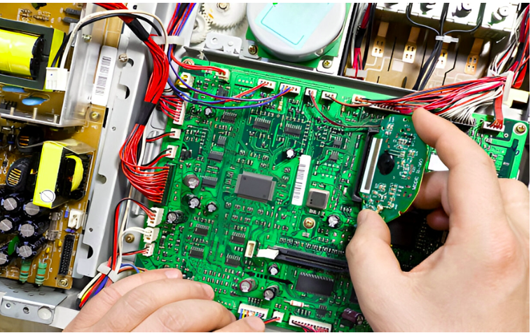
Telecom PCB assembly refers to the process of manufacturing and assembling printed circuit boards specifically designed for use in telecommunications equipment and infrastructure. These boards are the electronic backbone of devices and systems that transmit, receive, and process communication signals.
Unlike standard consumer electronics PCBs, telecom PCBs are engineered to meet much stricter performance, durability, and reliability standards. They are found in a wide variety of applications — from home routers and smartphones to base stations, satellite communication systems, and fiber optic networks.
Simply put, without telecom PCB assembly, the modern connected world as we know it would not exist.
Where Are Telecom PCBs Used?
Telecom PCBs are used across virtually every segment of the telecommunications industry. Here are some of the most common applications:
Network Infrastructure: Base transceiver stations (BTS), routers, switches, and optical fiber transmission systems all rely on high-performance PCBs to manage enormous volumes of data traffic reliably and without interruption.
Mobile Devices: Smartphones, tablets, and wearables contain multiple PCBs that handle everything from wireless signal processing to power management and audio output.
Broadband Equipment: DSL modems, cable modems, and fiber-optic terminal equipment use specialized PCBs to deliver fast and stable internet connections to homes and businesses.
Satellite Communication: Ground stations and onboard satellite electronics depend on rugged, high-frequency PCBs capable of operating in extreme environments.
Enterprise Communication Systems: Office phone systems, video conferencing equipment, and unified communication platforms all incorporate telecom-grade PCBs to ensure consistent performance.
What Makes Telecom PCBs Different?
Not all PCBs are created equal. Telecom PCBs have several characteristics that set them apart from boards used in everyday consumer products:
High-Frequency Performance: Telecom systems operate at high frequencies, often in the gigahertz (GHz) range. PCBs used in these systems must be able to handle high-speed signals without significant loss or interference. This requires the use of specialized low-loss materials like PTFE (polytetrafluoroethylene) or Rogers laminates.
Multi-Layer Construction: To pack more functionality into a smaller footprint, telecom PCBs often use multiple layers — sometimes 10, 20, or even more. Each layer carries different signals or power, and precise alignment during manufacturing is critical.
Thermal Management: Telecom equipment often runs continuously, generating significant heat. PCBs must be designed and assembled with effective heat dissipation in mind, using thermal vias, heat spreaders, or specialized materials.
Signal Integrity: Maintaining the accuracy and clarity of signals across the board is essential. Even minor manufacturing defects can introduce noise or signal loss that disrupts communication.
Durability and Longevity: Telecom infrastructure is expected to operate 24/7 for years, sometimes decades. The PCBs within these systems must be built to last, with robust solder joints, high-quality components, and protection against environmental factors like humidity, temperature changes, and vibration.
The Telecom PCB Assembly Process
The assembly of telecom PCBs follows a carefully controlled process to ensure every board meets the high standards required:
Design and Engineering Review: Before manufacturing begins, the PCB design is reviewed for manufacturability and compliance with telecom standards. Any issues with trace widths, signal paths, or component placement are identified and resolved early.
Material Selection: Given the performance demands of telecom applications, material selection is critical. High-frequency laminates, specific copper weights, and surface finishes are chosen based on the board’s intended use.
Bare Board Fabrication: The PCB layers are etched, drilled, and laminated together to create the bare board. For multi-layer telecom boards, this is a complex process requiring high precision.
Solder Paste Application: Solder paste is applied to the board’s surface pads using a stencil, preparing them to receive surface-mount components.
Component Placement: Automated pick-and-place machines position hundreds or even thousands of tiny components onto the board with remarkable speed and accuracy. For telecom boards, this often includes fine-pitch ICs, RF components, and high-speed connectors.
Reflow Soldering: The board passes through a reflow oven where the solder paste melts and forms permanent electrical connections between components and the board.
Inspection and Testing: Given the critical nature of telecom applications, quality control is extensive. Automated Optical Inspection (AOI), X-ray inspection for hidden solder joints, and in-circuit testing are commonly used. Functional testing simulates real-world operating conditions to verify performance.
Conformal Coating (if required): For boards destined for outdoor or harsh environments, a protective conformal coating may be applied to shield against moisture, dust, and chemical exposure.
Key Challenges in Telecom PCB Assembly
Assembling PCBs for telecom applications is not without its challenges:
Miniaturization: As telecom devices get smaller and more powerful, components are getting tinier and more densely packed. This pushes the limits of assembly precision and increases the risk of defects.
Regulatory Compliance: Telecom equipment must comply with a range of international standards and certifications, such as IPC-A-610, RoHS, and various regional telecom regulatory requirements. Assembly providers must stay current with these evolving requirements.
Supply Chain Complexity: Telecom PCBs often require specialty components with long lead times. Managing the supply chain effectively is essential to keeping production on schedule.
Evolving Technology: With the rapid rollout of 5G networks and the growing demand for faster, more reliable communication, telecom PCB designs are constantly evolving. Assembly providers must invest in the latest equipment and expertise to keep pace.
Choosing the Right Telecom PCB Assembly Partner
When selecting an assembly partner for telecom applications, consider the following:
- Experience with high-frequency and multi-layer boards
- Certifications such as ISO 9001, IPC-A-610, and UL
- Advanced inspection and testing capabilities
- Strong component sourcing network
- Proven track record with telecom clients
The right partner doesn’t just assemble boards — they understand the technical demands of telecom applications and work with you to ensure every board performs flawlessly in the field.
Conclusion
As the world becomes increasingly connected through 5G, IoT, and next-generation broadband, the demand for high-quality telecom PCB assembly will only continue to grow. From the smallest smartphone component to the largest network infrastructure equipment, reliable PCB assembly is what keeps our communications running smoothly. If you’re looking to source boards for telecom applications, partnering with an experienced China telecom PCB assembly provider can offer the combination of technical expertise, advanced manufacturing capabilities, and cost efficiency that modern telecom projects demand.